Perovskite Nanostructures for Optoelectronics and Fundamental Studies
Metal halide perovskites have recently re-emerged as a new class of earth-abundant semiconductor materials that have exceptional promise for solar cells and other optoelectronic applications including light-emitting diodes (LED), lasers, and (X-ray) photodetectors. Despite exciting progress of device performance in thin films, perovskite nanostructures, such as 1D nanowires, would create new opportunities for controlling light absorption, charge transport, charge separation and recombination that are crucial in solar cells and other optoelectronic devices. Our research interests focus on (1) rational design, synthesis, and characterizations of single-crystal nanostructures of the diverse families of perovskite materials with different compositions and dimensionalities with different properties; (2) perovskite nanostructures as building blocks for nanoscale optoelectronics and photonics; (3) diverse perovskite nanostructures as model systems to investigate their fundamental physical properties.
Solution Growth of Perovskite Nanostructures
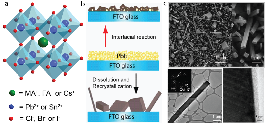
Understanding crystal growth and improving material quality is important for improving semiconductors for electronic, optoelectronic, and photovoltaic applications. We first revealed mechanistic insights on the crystal growth of perovskite nanostructures using a facile solution conversion from lead precursor films to perovskites.1 Such conversion growth involves two possible pathways, an interfacial reaction process or a dissolution-recrystallization process, whose relative importance depends on the halide concentration of precursor solution (Figure 1).
Fast interfacial reaction:
PbI2 (s) + CH3NH3+ (sol) + I- (sol) → CH3NH3PbI3 (s)
Slow dissolution-recrystallization pathway:
PbI2 (s) + 2I- (sol) → PbI42- (sol)
PbI42- (sol) + CH3NH3+ (sol) → CH3NH3PbI3 (s) + I-(sol)
Following the dissolution-recrystallization growth mechanism, we found that the key to successful growth of single-crystal nanowires, nanorods, and nanoplates of APbX3 [A = methylammonium (MA), formamidinium (FA), or Cs; X = Cl, Br, or I] is the slow release of the low-concentration Pb precursor from the precursor film on the substrate and the careful tuning of the halide precursor concentration to maintain a low supersaturation condition for perovskite crystal growth.2-4

Figure 1. (a) The schematic crystal structure of lead halide perovskites ABX3. (b) Illustrations of the two growth mechanisms of crystalline perovskite nanostructures. (c) SEM and TEM images of some example perovskite NWs.
Two-dimensional (2D) layered perovskites with a general formula of (RNH3)2An-1BnX3n+1 (R is a long-chain alkyl or aromatic group) can be formed by slicing the 3D cubic perovskites along crystallographic (100) plane through incorporating a long-chain ammonium cation (RX). These 2D perovskites have intrinsic quantum confinements due to the nanoscale thick semiconductor layers separated by dielectric layers. Following our understanding on the crystal growth, we further developed a solution-phase transport-growth process (Figure 2) to synthesize single-crystal microplates of 2D layered perovskites with a well-defined rectangular geometry and nanoscale thickness that are suitable building blocks for integrated optoelectronics and (nano)photonics.5

Figure 2. Microplates of 2D perovskite (PEA)2PbX4 grown via a solution-transport process.
Vapor Phase Epitaxial Growth of All-Inorganic Perovskites
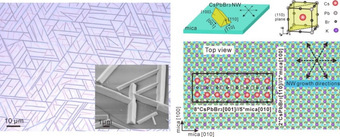
We have also developed the growth of high-quality crystalline inorganic halide perovskites with controllable morphologies and growth directions that will be more convenient for optoelectronic device applications. In general, hybrid perovskites (i.e. MAPbI3) are not very friendly for high-temperature vapor-phase growth because of their poor thermal stability, but vapor-phase synthesis is a good choice for growing inorganic perovskites with improved crystal quality because they are thermally stable at moderately high temperatures. We have developed a vapor-phase epitaxial growth of horizontal single-crystal CsPbX3 (X = Cl, Br, I) nanowires and microwires (MWs) with controlled crystallographic orientations on the (001) plane of phlogopite and muscovite mica (Figure 3).6 We proposed an incommensurate heteroepitaxial lattice match between the CsPbBr3 and mica crystal structures and the growth mechanism of these horizontal wires was due to asymmetric lattice mismatch. These well-connected NWs network could serve as straightforward platforms for fundamental studies and optoelectronic applications.

Figure 3. (a) Optical image of vapor-phase grown horizontally aligned CsPbBr3 on mica (001). (b) Schematic illustration of the epitaxial mechanism of CsPbBr3 NWs on mica (001)
High-quality single crystals have low defect densities and excellent photophysical properties, yet thin films are the most sought after material geometry for optoelectronic devices. Perovskite single-crystal thin films (SCTFs) would be highly desirable for high performance devices, but their growth remains challenging, particularly for inorganic halide perovskites. We have also reported a facile vapor-phase epitaxial growth of cesium lead bromide perovskite (CsPbBr3) continuous SCTFs with controllable micrometer thickness, as well as nanoplate arrays, on traditional oxide perovskite SrTiO3 (100) substrates (Figure 4).7 Heteroepitaxial single-crystal growth is enabled by the serendipitous incommensurate lattice match between these two perovskites and overcoming the limitation of island forming Volmer-Weber crystal growth is critical for growing large-area continuous thin films. Our work suggests a general approach using oxide perovskites as substrates for heteroepitaxial growth of halide perovskites. The high-quality halide perovskite SCTFs epitaxially integrated with multifunctional oxide perovskites could open up opportunities for a variety of high-performance optoelectronics devices.

Figure 4. Vapor-phase growth of CsPbBr3 nanoplate arrays and continuous thin films on traditional oxide perovskite SrTiO3 (100) substrates, together with schematic illustration of the incommensurate lattice match between CsPbBr3 (100) and STO (100) crystallographic planes.
Controlling Metastability of Metal Iodide Perovskites
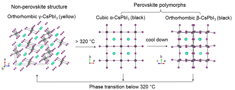
Metastable structural polymorphs can have superior properties and applications than their thermodynamically stable phases but rational synthesis of metastable phases is a challenge. For example, due to the ionic mismatch as reflected by the Goldsmidt structural tolerance factor, the perovskite structures of FAPbI3 and CsPbI3 that hold great promises in solar and light-emitting applications are metastable at room temperature (see Figure 5 for an example of different polymorphs of CsPbI3 and their phase transitions).8,9 The spontaneous phase transitions not only rule out the possible use of these metastable perovskite phases in practical applications, but also prevents the study of the intrinsic photophysical properties.

Figure 5. Crystal structures of different perovskite and non-perovskite polymorphs of CsPbI3 and the phase transitions between them.
We have developed a thermal quenching or an ion exchange method to gain access to the metastable phase of these nanostructures kinetically.3,4 In addition, making alloyed perovskites can stabilize the perovskite phases thermodynamically.3 More importantly, we have also developed a new chemical strategy based on surface ligand functionalization during direct solution growth to stabilize the metastable pure lead iodide perovskite nanostructures and thin films (Figure 6).8,9 The surface functionalization can reduce the surface energy and promote the crystal growth of metastable perovskite phase both thermodynamically and kinetically, demonstrating the importance of surface chemistry on the phase stability of perovskite materials. These stabilized iodide perovskites showed phase stability over months. This discovery has not only enabled the practical optoelectronic applications of metastable perovskites, but also provide new insights on the control of metastable structural polymorphs and manipulating the thermodynamic phase stability of solid state materials in general.

Figure 6. (a) Schematic illustration and structural characterizations of the different perovskite products grown under the presence of long-chain ammonium cations (LA) with various LA/FA molar ratios. (b, c, d) SEM images of the hexagonal FAPbI3, cubic FAPbI3, and layered perovskite (LA)2(FA)Pb2I7
High-Performance Perovskite Nanowire Lasers
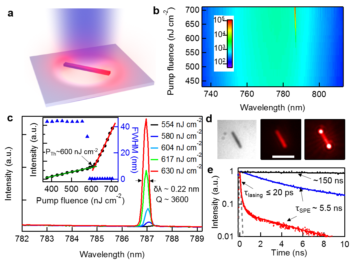
The remarkable performance of lead halide perovskites in solar cells can be attributed to the long carrier lifetimes and low non-radiative recombination rates, the same physical properties that are ideal for semiconductor lasers. In collaboration with Prof. Xiaoyang Zhu’s group, we showed room temperature and wavelength tunable lasing from single-crystal methylammonium lead halide perovskite NWs (Figure 4) with very low lasing thresholds (~ 102 nJ/cm2) and high quality factors (Q ~ 3600),2 which are much better than that of any other semiconductor NW lasers previously reported. Kinetic analysis based on time-resolved fluorescence reveals little charge carrier trapping in these single-crystal NWs and gives estimated lasing quantum yields approaching 100%.2 Furthermore, the NW lasers of all-inorganic perovskites (i.e. CsPbBr3) show stable lasing emission with no measurable degradation after at least 8 hours or 7.2×10⁹ laser shots under continuous illumination,4 which are substantially more robust than their organic-inorganic counterparts.3 Such lasing performance, coupled with facile solution phase growth of single-crystal NWs and broad tunability of emission color from 410 nm to 820 nm using different cation and anion stoichiometry (Figure 5), makes lead halide perovskites ideal materials for the development of nano-photonics and optoelectronic devices.

Figure 7. Optically-pumped lasing from single-crystal MAPbI3 NWs. (a) Schematic of a NW pumped by 402 nm laser excitation. (b) 2D pseudo-color plot of NW emission spectra under different pump fluences (P) showing a broad SPE peak below the threshold (PTh) of 600 nJ cm-2 and a narrow lasing peak above the threshold. (c) NW emission spectra around the lasing threshold. Inset is integrated emission intensity and FWHM as a function of P. (d) Optical image of single NW. The middle and right images show the NW emission below and above PTh. The emission is uniform below PTh but mostly comes from the two end facets with coherent interference under lasing operation. (e) TRPL decay kinetics after photoexcitation with fluence below and above the threshold.

Figure 8. (a) Broad tunable lasing emission wavelength at room temperature from various perovskite NWs with different cations and anions. (b) Fluorescence images of perovskite NWs lasers with different colors above the lasing threshold.
2D Layered Perovskite Nanoplates for Light-Emitting Diodes
Lead halide perovskites are also very promising LED materials, but the efficiency of the blue-color LED devices has remained poor. Transitioning from 3D perovskites into 2D layered structures introduce quantum confinement effects in these materials, and, therefore, 2D perovskites are expected to display wider band gaps, narrower photoluminescence (PL) peaks, and higher PL quantum yield efficiency as compared to their 3D analogues, which makes them more promising for display and lighting application. We collaboratively demonstrated a color-pure, room-temperature-operable violet LED using (PEA)2PbBr4 as the luminescent layer (Figure 6), which is the first non-inorganic LED with violet color. The LED displayed a narrow electroluminescence peak centered at 410 nm, with a fwhm of 14 nm.10 Critical to this success is a solvent vapor annealing technique that converted as-deposited polycrystalline thin film into high-quality micrometer-sized nanoplates, which enhances both the photophysical properties of this 2D perovskite and the external quantum efficiency.

Figure 9. (a) Crystal structure of 2D perovskite PEA2PbBr4. (b) Schematic illustrations of the solvent vapor annealing technique. (c) EQE for the LED devices fabricated with thin film and nanoplates. (d) EL spectra of a typical LED device in comparison with the PL spectra. Inset is cross-sectional SEM image of the device.
Perovskite Nanostructures for Fundamental Studies
These single-crystal perovskite nanostructures are ideal model systems for fundamental studies and as convenient building blocks for proof-of-principle studies of optoelectronic device design and improvement.11-15 We have been collaborating with many research groups to study the fundamental properties of perovskites. For example, our collaborator Prof. Xiaoyang Zhu at Columbia University recently revealed the carrier protection mechanism by comparing nanoplates of three lead bromide perovskites: MAPbBr3, FAPbBr3, and CsPbBr3. Specifically, hot fluorescence emission from energetic carriers with ~102 ps lifetimes was observed in MAPbBr3 and FAPbBr3, but not in CsPbBr3, suggesting energetic carriers in hybrid perovskites are protected by the molecular reorientational motion of organic cations.11 Moreover, the three samples show similar band edge carrier dynamics, suggesting the long-lived charges can be efficiently screened in the intrinsic soft lead halide perovskite structure, regardless of A-site cation.12 Our collaborator Prof. Dong Yu at the University of California at Davis employed scanning photocurrent microscopy (SPCM) measurements on single-crystal MAPbI3 nanostructures to find a minority charge carrier diffusion length up to 21 μm, which is significantly longer than the values observed in polycrystalline film.13 Here in Madison, we have also been collaborating with Prof. John Wright and Prof. Randall Goldsmith’s groups to study the carrier decay photophysics of MAPbI314 and the dependence the photophysical properties on the compositions and structures of mixed-cation and anion perovskites.15

Figure 10. (a, b) Pseudocolor plot of TR-PL spectra for a FAPbBr3 nanoplate and a CsPbBr3 nanoplate. (c) Photocurrent mapping of a MAPbI3 nanowire device
Collaborators
Prof. Xiaoyang Zhu http://www.columbia.edu/cu/chemistry/groups/zhu/
Prof. Dong Yu http://yu.physics.ucdavis.edu/
Prof. John Wright http://wright.chem.wisc.edu/
Prof. Randall Goldsmith http://goldsmith.chem.wisc.edu/
1) Yongping Fu, Fei Meng, Matthew B. Rowley, Blaise J. Thompson, Melinda J. Shearer, Dewei Ma, Robert J Hamers, John C. Wright, and Song Jin, Solution Growth of Single Crystal Methylammonium Lead Halide Perovskite Nanostructures for Optoelectronic and Photovoltaic Applications, J. Am. Chem. Soc, 2015, 137(17), pp 5810-5818, DOI: 10.1021/jacs.5b02651
2) Haiming Zhu, Yongping Fu, Fei Meng, Xiaoxi Wu, Zizhou Gong, Qi Ding, Martin V. Gustafsson, M. Tuan Trinh, Song Jin & X-Y. Zhu, Lead halide perovskite nanowire lasers with low lasing thresholds and high quality factors, Nature Materials, 2015,14, 636. DOI: 10.1038/nmat4271
3) Yongping Fu, Haiming Zhu, Alex W. Schrader, Dong Liang, Qi Ding, Prakriti Joshi, Leekyoung Hwang, X-Y. Zhu, and Song Jin, Nanowire Lasers of Formamidinium Lead Halide Perovskites and Their Stabilized Alloys with Improved Stability, Nano Lett., 2016, 16, 1000-1008, DOI: 10.1021/acs.nanolett.5b04053
4) Yongping Fu, Haiming Zhu, Constantinos C. Stoumpos, Qi Ding, Jue Wang, Mercouri G. Kanatzidis, Xiaoyang Zhu, and Song Jin, Broad Wavelength Tunable Robust Lasing from Single-Crystal Nanowires of Cesium Lead Halide Perovskites (CsPbX3, X=Cl, Br, I), ACS Nano, 2016, 10, 7963–7972, DOI: 10.1021/acsnano.6b03916
5) Dewei Ma, Yongping Fu, Lianna Dang, Jianyuan Zhai, Ilia A. Guzei, and Song Jin, Single-crystal microplates of two-dimensional organic-inorganic lead halide layered perovskites for optoelectronics, Nano Research, 2017, 10, 2117-2129. DOI: 10.1007/s12274-016-1401-6
6) Jie Chen, Yongping Fu, Leith Samad, Lianna Dang, Yuzhou Zhao, Shaohua Shen, Liejin Guo, and Song Jin, Vapor-Phase Epitaxial Growth of Aligned Nanowire Networks of Cesium Lead Halide Perovskites (CsPbX3, X = Cl, Br, I), Nano Lett., 2017, 17, 460–466, DOI: 10.1021/acs.nanolett.6b04450
7) Jie Chen, Darien Morrow, Yongping Fu, Weihao Zheng, Yuzhou Zhao, Lianna Dang, Matthew John Stolt, Daniel D. Kohler, Xiaoxia Wang, Kyle J. Czech, Matthew P. Hautzinger, Shaohua Shen, Liejin Guo, Anlian Pan, John C. Wright, and Song Jin, Single-Crystal Thin Films of Cesium Lead Bromide Perovskite Epitaxially Grown on Metal Oxide Perovskite (SrTiO3), J. Am. Chem. Soc., 2017, 139, 13525-13532, DOI: 10.1021/jacs.7b07506
8) Yongping Fu, Tao Wu, Jue Wang, Jianyuan Zhai, Melinda J. Shearer, Yuzhou Zhao, Robert J Hamers, Erjun Kan, Kaiming Deng, Xiaoyang Zhu, and Song Jin, Stabilization of the Metastable Lead Iodide Perovskite Phase via Surface Functionalization, Nano Lett., 2017, 17, 4405–4414, DOI: 10.1021/acs.nanolett.7b01500
9) Yongping Fu, Morgan T. Rea, Jie Chen, Darien Morrow, Matthew P. Hautzinger, Yuzhou Zhao, Dongxu Pan, Lydia H. Manger, John C. Wright, Randall H. Goldsmith, and Song Jin, Selective Stabilization and Photophysical Properties of Metastable Perovskite Polymorphs of CsPbI3 in Thin Films, Chem. Mater., 2017, 29, 8385–8394, DOI: 10.1021/acs.chemmater.7b02948
10) Dong Liang, Yuelin Peng, Yongping Fu, Melinda J. Shearer, Jingjing Zhang, Jianyuan Zhai, Yi Zhang, Robert J. Hamers, Trisha L. Andrew, and Song Jin, Color-Pure Violet-Light-Emitting Diodes Based on Layered Lead Halide Perovskite Nanoplates, ACS Nano, 2016, 10, 6897–6904, DOI: 10.1021/acsnano.6b02683
11) Haiming Zhu, Kiyoshi Miyata, Yongping Fu, Jue Wang, Prakriti P. Joshi, Daniel Niesner, Kristopher W. Williams, Song Jin, Xiaoyang Zhu, Screening in crystalline liquids protects energetic carriers in hybrid perovskites, Science, 2016, 353, 1409-1413. DOI: 10.1126/science.aaf9570
12) Haiming Zhu, M. Tuan Trinh, Jue Wang, Yongping Fu, Prakriti P. Joshi, Kiyoshi Miyata, Song Jin, X.-Y. Zhu, Organic Cations Might Not Be Essential to the Remarkable Properties of Band Edge Carriers in Lead Halide Perovskites, Adv. Mater. 2017, 29, 1603072, DOI: 10.1002/adma.201603072
13) Rui Xiao, Yasen Hou, Yongping Fu, Xingyue Peng, Qi Wang, Eliovardo Gonzalez, Song Jin, and Dong Yu, Photocurrent Mapping in Single-Crystal Methylammonium Lead Iodide Perovskite Nanostructures, Nano Lett., 2016, 16, 7710–7717, DOI: 10.1021/acs.nanolett.6b03782
14) Lydia H. Manger, Matthew B. Rowley, Yongping Fu, Alexander K. Foote, Morgan T. Rea, Sharla L Wood, Song Jin, John C. Wright, and Randall H. Goldsmith, Global Analysis of Perovskite Photophysics Reveals Importance of Geminate Pathways, J. Phys. Chem. C, 2017, 121, 1062–1071, DOI: 10.1021/acs.jpcc.6b11547
15) Jun Dai, Yongping Fu, Lydia H. Manger, Morgan T. Rea, Leekyoung Hwang, Randall H. Goldsmith, and Song Jin, Carrier Decay Properties of Mixed Cation Formamidinium-Methylammonium Lead Iodide Perovskite [HC(NH2)2]1-x[CH3NH3]xPbI3 Nanorods, J. Phys. Chem. Lett., 2016, 7, 5036–5043, DOI: 10.1021/acs.jpclett.6b01958
16) Xuelu Hu, Hong Zhou, Zhenyu Jiang, Xiao Wang , Shuangping Yuan, Jianyue Lan, Yongping Fu , Xuehong Zhang, Weihao Zheng, Xiaoxia Wang, Xiaoli Zhu, Lei Liao, Gengzhao Xu, Song Jin, and Anlian Pan, Direct Vapor Growth of Perovskite CsPbBr3 Nanoplate Electroluminescence Devices, ACS Nano, 2017, 11 , 9869–9876, DOI: 10.1021/acsnano.7b03660
17) Meiying Leng, Ying Yang, Kai Zeng, Zhengwu Chen, Zhifang Tan, Shunran Li, Jinghui Li, Bing Xu, Dengbing Li, Matthew P. Hautzinger, Yongping Fu, Tianyou Zhai, Ling Xu, Guangda Niu, Song Jin and Jiang Tang, All-Inorganic Bismuth-Based Perovskite Quantum Dots with Bright Blue Photoluminescence and Excellent Stability, Adv. Funct. Mater., 2017, 28, 1704446. DOI: 10.1002/adfm.201704446
18) Matthew P. Hautzinger, Jun Dai, Yujin Ji, Yongping Fu, Jie Chen, Ilia A. Guzei, John C. Wright, Youyong Li and Song Jin, Two-Dimensional Lead Halide Perovskites Templated by a Conjugated Asymmetric Diammonium, Inorg. Chem., 2017, 56, 14991–14998, DOI: 10.1021/acs.inorgchem.7b02285
19) Tyler J. S. Evans, Andrew Schlaus, Yongping Fu, Xinjue Zhong, Timothy L. Atallah, Michael S. Spencer, Louis E. Brus, Song Jin and X.-Y. Zhu, Continuous-Wave Lasing in Cesium Lead Bromide Perovskite Nanowires, Adv. Opt. Mater., 2018, 6, 1700982, DOI: 10.1002/adom.201700982
20) Dongxu Pan, Yongping Fu, Jie Chen, Kyle J. Czech, John C. Wright, and Song Jin, Visualization and Studies of Ion Diffusion Kinetics in Cesium Lead Bromide Perovskite Nanowires, Nano Lett., 2018, 18, 1807–1813. DOI: 10.1021/acs.nanolett.7b05023
21) Meiying Leng, Ying Yang, Zhengwu Chen, Wanru Gao, Jian Zhang, Guangda Niu, Dengbing Li, Haisheng Song, Jianbing Zhang, Song Jin, and Jiang Tang, Surface Passivation of Bismuth-Based Perovskite Variant Quantum Dots To Achieve Efficient Blue Emission, Nano Lett. 2018, 18, 6076–6083 DOI: 10.1021/acs.nanolett.8b03090
22) Yongping Fu, Weihao Zheng, Xiaoxia Wang, Matthew P. Hautzinger, Dongxu Pan, Lianna Dang, John C. Wright, Anlian Pan, and Song Jin, Multicolor Heterostructures of Two-Dimensional Layered Halide Perovskites that Show Interlayer Energy Transfer, J. Am. Chem. Soc., 2018, 140, 15675–15683. DOI: 10.1021/jacs.8b07843
23) Yongping Fu, Haiming Zhu, Jie Chen, Matthew P. Hautzinger, X.-Y. Zhu and Song Jin, Metal halide perovskite nanostructures for optoelectronic applications and the study of physical properties, Nature Reviews Materials, 2019, 4,169-188. DOI: 10.1038/s41578-019-0080-9
24) Jie Chen, Ziyu Luo, Yongping Fu, Xiaoxia Wang, Kyle J. Czech, Shaohua Shen, Liejin Guo, John C. Wright, Anlian Pan, and Song Jin, Tin(IV)-Tolerant Vapor-Phase Growth and Photophysical Properties of Aligned Cesium Tin Halide Perovskite (CsSnX3; X = Br, I) Nanowires, ACS Energy Lett., 2019, 4, 1045–1052. DOI: 10.1021/acsenergylett.9b00543
25) Tiefeng Yang, Xiao Wang, Biyuan Zheng, Zhaoyang Qi, Chao Ma, Yuhao Fu, Yongping Fu, Matthew P. Hautzinger, Ying Jiang, Ziwei Li, Peng Fan, Fang Li, Weihao Zheng, Ziyu Luo, Jie Liu, Bin Yang, Shula Chen, Dong Li, Lijun Zhang, Song Jin, and Anlian Pan. Ultrahigh-Performance Optoelectronics Demonstrated in Ultrathin Perovskite-Based Vertical Semiconductor Heterostructures. ACS Nano, 2019, Advance online publication. DOI: 10.1021/acsnano.9b02676
26) Yongping Fu, Matthew P. Hautzinger, Ziyu Luo, Feifan Wang, Dongxu Pan, Michael M. Aristov, Ilia A. Guzei, Anlian Pan, Xiaoyang Zhu and Song Jin. Incorporating Large A Cations into Lead Iodide Perovskite Cages: Relaxed Goldschmidt Tolerance Factor and Impact on Exciton–Phonon Interaction. ACS Cent. Sci. 2019, Advance online publication. DOI: 10.1021/acscentsci.9b00367
